From Sand to Silicon
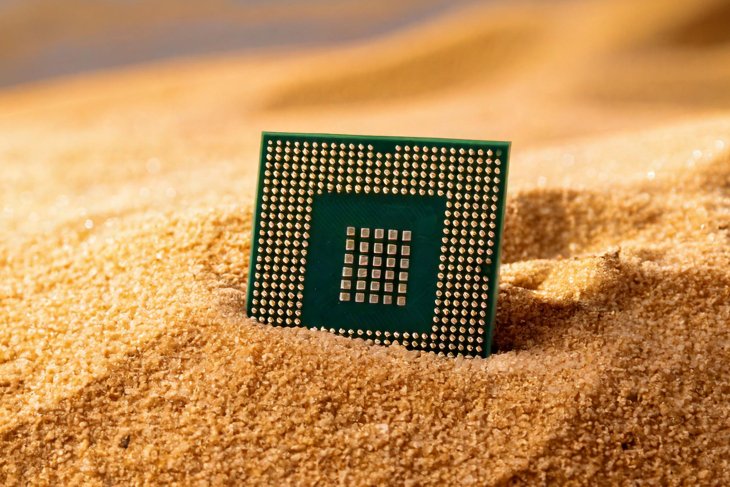
Every electronic device runs on silicon chips that begin as ordinary sand.
In nature, silicon is locked up in quartz (silicon dioxide, SiO₂) sand – about 95% of common quartz sand is SiO₂. To make chips, manufacturers first purify this sand. They heat quartz with carbon in a furnace, driving off oxygen and leaving raw metallurgical-grade silicon. Next, a chemical refining step (the Siemens process) turns this into polysilicon: ultra-pure polycrystalline silicon with impurity levels below a few parts per billion en.wikipedia.org. These purified silicon rods (polysilicon) are the feedstock for crystal growth._____________________________________________________________________________
Crystal Growth: Pulling a Single Crystal :
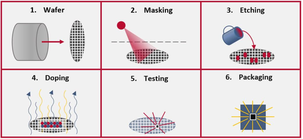
The polysilicon feedstock is melted and a tiny seed crystal is slowly pulled upward, in what’s called the Czochralski process en.wikipedia.org. As the seed emerges, it drags a large, cylindrical single-crystal silicon boule (ingot) out of the melt. The ingot can be over a meter long and weighs hundreds of pounds. Once cooled, the boule is precisely sliced into circular wafers – think of slicing a log into thin discs. Common wafer diameters today are 100 mm, 150 mm, 200 mm or 300 mm. Larger wafers mean more chips per slice (for example, moving to a 300 mm wafer cut cost per chip by 30–40%). Each new wafer is then polished on both sides until it is mirror-smooth and perfectly flat.Wafer Slicing and Polishing :
The silicon boule is secured on a jig and cut with a high-speed diamond saw. Each cut yields a wafer only a few hundred microns thick (roughly 0.5 mm). After slicing, any sawing damage is removed: the wafer is lapped and polished to a mirror finish. This polished wafer is now ready for circuit fabrication. (Each wafer can hold anywhere from dozens to thousands of chips, depending on chip size asml.com :)
Photolithography & Doping :
With a blank wafer prepared, the next step is photolithography – using light to transfer circuit patterns onto the silicon en.wikipedia.org. First, the wafer is coated with a light-sensitive polymer called photoresist. A glass mask (with the desired circuit pattern) is aligned over the wafer, and ultraviolet light is shone through it. Wherever the light hits, the photoresist’s chemistry changes. After exposure, the wafer is developed: the altered resist is washed away (in a positive-resist process), leaving a stencil of the pattern. An etching process then removes the exposed silicon or oxide in those areas, carving the pattern into the wafer. The remaining resist is stripped away, leaving the patterned wafer surface.
Typically, modern chips require many stacked layers. A single wafer may go through dozens of these lithography/etch cycles en.wikipedia.org, building up layers of transistors and wiring. Between pattern steps, the wafer is often doped with impurities to create semiconductor regions. For example, boron atoms (with 3 valence electrons) are diffused in to make p-type regions, and phosphorus (5 valence electrons) for n-type en.wikipedia.org. Just a few impurity atoms among billions can dramatically change silicon’s conductivity. This intentional doping controls where transistors will conduct electricity, forming the p–n junctions at the heart of every chip.
Metallization & Packaging :
Once all the transistor structures are defined, the wafer needs metal wires to connect them. In a step called metallization, ultra-thin layers of metal (commonly aluminum or copper) are vacuum-deposited onto the waferosha.gov. These layers are also patterned by photolithography/etch to form the interconnect wiring. Finally, each wafer is tested for functionality, then diced into individual chips (dies) using a precision diamond saw asml.com. Each chip die is picked and placed on a package substrate (a small PCB or lead frame). Tiny bond wires or solder bumps link the die to the external pins. A small metal “heat spreader” or lid is often attached on top to help carry away heat asm.com. The chip is then sealed in a protective housing to guard against moisture and mechanical stress. After final testing, the packaged chips (complete with leads or balls) are ready to be soldered onto circuit boards and put to work.
_____________________________________________________________________
Try It Yourself: Kits and Resources :
If this journey sparked your curiosity, there are plenty of ways to get hands-on. Hobbyist electronics starter kits provide the components and guides you need to begin building simple circuits (for example, the Arduino Starter Kit)https://amzn.to/4daH8J0.You can even buy a polished silicon wafer https://amzn.to/4m2YX0l(used as tech-art or for education) and inspect the transistor patterns under magnification. A good microscope kit(e.g. the AmScope 120×–1200× Beginner Microscope) https://amzn.to/44YeF6R will let you see circuit details on a chip. And if you want to learn the design side, books like HDL Chip Design https://amzn.to/434l2TR
Each of these steps – from sand to polished silicon to the tiny chip in your device – is a marvel of engineering. By understanding the process, we can better appreciate how the gadgets in our pockets are made, and maybe even start making our own DIY electronics along the way.


Comments
Post a Comment